Nmos Diagram Pmos Nmos Transistor
Nmos inverter circuit diagram Nmos inverter in vlsi Cmos vs mosfet
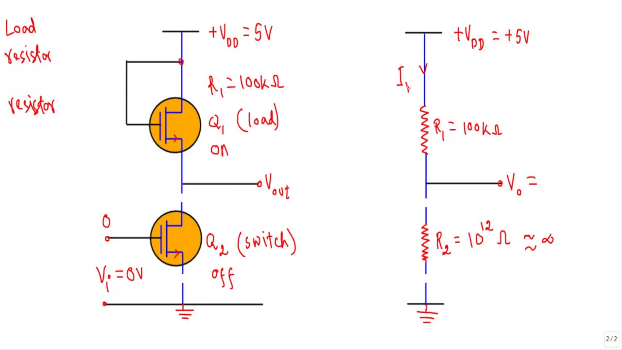
Nmos Schematic Diagram
Nmos inverter circuit consists calculate nml enhancement transistors Introduction to nmos and pmos transistors Nmos schematic diagram
Brief review of the structure of mos transistors
Lec28d deriving nmos transfer characteristicsCircuit diagram of nmos and pmos Nmos transistorNmos and pmos symbol.
Pmos nmos transistor cmos transistors circuit connectedConsider the following nmos inverter circuit which consists of two 1 diagram of nmos with four terminals: gate, drain, source and bodyCmos transistor symbol.

Mosfet transistors mos terminal body schematic electronic electronics tutorial devices diodes
Latch nmos cross sectionMosfet || electronics tutorial Cmos transistor symbolNmos cross section area with body biased. fig (3) and fig (4) shows a.
Download nmos and stick diagramMos transistors brief rahsoft Nmos transistorNmos transistor structure diode does mosfet cmos two diagram interconnecting relate its transistors electronics failure stackexchange questions analysis stack.

The symbol of (a) a pmos transistor and (b) an nmos transistor
Nmos transistor layout mos section cross ppt powerpoint presentation substrate electrical body sourcePmos nmos transistors Solved basic nmos diagram: given g is conducting, when canNmos structure.
Ohne verbunden serviette transistor mos tennis herrin lolNmos schematic 01 openclipart images Cross section of the pmos and nmos transistor.Nmos transistor layout with a deep n-well.
Mosfet diagram circuit working principle basics basic deflection mode example applications electronics transistor switch switching elprocus high choose board
Pmos nmos transistorNmos inverter circuit What is the mosfet: basics, working principle and applicationsNmos structure physical ppt powerpoint presentation skip video slideserve.
Nmos stick diagramMosfet physics Pmos circuit diagramInverter nmos circuit.

Nmos schematic layout lab 421l lab8
Nmos schematic diagramNmos and pmos transistors structure .
.


